Market of 3D electronics is forecast to grow to US$4.3 bn by 2034.
3D Electronics/Additive Electronics 2024-2034: Technologies, Players, and Markets
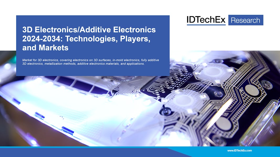
Market for 3D electronics, covering electronics on 3D surfaces, in-mold electronics, fully additive 3D electronics, metallization methods, additive electronics materials, and applications.
Show All
Description
Contents, Table & Figures List
Pricing
Related Content
IDTechEx's report "3D Electronics/Additive Electronics 2024-2034: Technologies, Players, and Markets" analyses the technologies and market trends that promise to bring electronics into the 3D realm. Drawing from over 40 company profiles, the majority based on interviews, it assesses three distinct segments of the 3D electronics landscape: applying electronics to a 3D surface (partially additive), in-mold electronics, and fully additive electronics. Within each segment, the report evaluates the different technologies, potential adoption barriers, and application opportunities. It includes detailed 10-year market forecasts for each technology and application sector, delineated by both revenue and area/volume.
Motivation for 3D electronics
While partially additive 3D electronics has long been used for adding antennas and simple conductive interconnects to the surface of 3D injection-molded plastic objects, more complex circuits are increasingly being added onto surfaces made from a variety of materials by utilizing new techniques. Furthermore, in-mold electronics and 3D printed electronics enable complete circuits to be integrated within an object, offering multiple benefits that include simplified manufacturing and novel form factors. With 3D electronics, adding electronic functionality no longer requires incorporating a rigid, planar PCB into an object then wiring up the relevant switches, sensors, power sources, and other external components.
The report weighs the pros and cons of each approach against each other for multiple applications, with numerous case studies showing how the different manufacturing techniques are deployed across the automotive, consumer goods, IC packaging and medical device sectors. Furthermore, through detailed analysis of the technologies and their requirements, IDTechEx identifies innovation opportunities for both materials and manufacturing methods.
Applying electronics to a 3D surface
The most established approach to adding electrical functionality onto the surface of 3D objects is laser direct structuring (LDS). LDS saw tremendous growth around a decade ago and is used to manufacture hundreds of millions of devices each year, around 75% of which are antennas. However, despite its high patterning speed and widespread adoption, LDS has some weaknesses that leave space for alternative approaches to surface metallization. Valve jet printing or termed dispensing, a technique enabling wide range of materials deposition, is already used for a small proportion of antennas, and is the approach of choice for systems that deposit entire circuits onto 3D surfaces.
Aerosol jetting and laser induced forward transfer (LIFT) are other digital deposition technologies, which offer higher resolutions and rapid deposition of a wide range of materials respectively. Other emerging techniques such as ultra precise dispensing, electrohydrodynamic printing, impulse printing, pad printing, spray metallization are also benchmarked in this report, enabling new market potential of electronics on 3D surfaces. An advantage of digital deposition methods of the incumbent LDS technology is that dielectric materials can also be deposited within the same printing system, thereby enabling multilayer circuits. Insulating and conductive adhesives can also deposited, enabling SMD components to be mounted onto the surface.

Status and market potential of metallization methods for each application. Source: IDTechEx
In-mold electronics
In-mold electronics (IME), in which electronics are printed/mounted prior to thermoforming into a 3D component, facilitates the transition towards greater integration of electronics, especially where capacitive touch sensing and lighting is required. IME offers multiple advantages relative to conventional mechanical switches, including reduction in weight and material consumption of up to 70% and much simpler assembly. The IME manufacturing process can be regarded as an extension of the well established in-mold decorating (IMD) process, thus much of the existing process knowledge and capital equipment can be reused. IME differs from IMD though the initial screen printing of conductive thermoformable inks, followed by deposition of electrically conductive adhesives and the mounting of SMDs (surface mount devices, primarily LEDs at present). More complex multilayer circuits can also be produced by printing dielectric inks to enable crossovers.
Despite the wide range of applications and the advantageous reductions in size, weight, and manufacturing complexity, commercial deployment of IME integrated SMD components has thus far been fairly limited. This relatively slow adoption, especially within the primary target market of automotive interiors, is attributed to both the challenges of meeting automotive qualification requirements and the range of less sophisticated alternatives such as applying functional films to thermoformed parts. Along with greater acceptance of the technology, this will require clear design rules, materials that conform to established standards, and crucially the development of electronic design tools.
Fully printed 3D electronics
The least developed technology is fully printed 3D electronics, in which dielectric materials and conductive materials are sequentially deposited. Combined with placed SMD components, this results in a circuit, potentially with a complex multilayer structure embedded in a 3D plastic object. The core value proposition is that each object and embedded circuit can be manufactured to a different design without the expense of manufacturing masks and molds each time. Fully 3D printed electronics are thus well suited to applications where a wide range of components need to be manufactured at short notice. The technology is also promising for applications where a customized shape and even functionality is important. The ability of 3D printed electronics to manufacture different components using the same equipment, and the associated decoupling of unit cost and volume, could also enable a transition to on-demand manufacturing.
The challenges for fully 3D printed electronics are that manufacturing is fundamentally a much slower process than making parts via injection molding since each layer needs to be deposited sequentially. While the printing process can be accelerated using multiple nozzles, it is best targeted at applications where the customizability offers a tangible advantage. Ensuring reliability is also a challenge, considering different material properties; additionally, with embedded electronics post-hoc repairs are impossible - one strategy is using image analysis to check each layer and perform any repairs before the next layer is deposited.
Comprehensive analysis and market forecasts
IDTechEx has been researching the emerging printed electronics market for well over a decade, launching our first printed and flexible sensor report back in 2012. Since then, we have stayed close to the technical and market developments, interviewing key players worldwide, attending numerous conferences, delivering multiple consulting projects, and running classes and workshops on the topic. This enables us to provide a complete picture of the 3D electronics technological and market landscape, along with the entire field of printed electronics.
This report provides the following information:
Technology trends & manufacturer analysis:
- Introduction to 3D electronics including electronics on 3D surfaces, in-mold electronics and fully additive electronics.
- Detailed technology benchmarking on conventional and emerging metallization methods.
- Discussion of the status, challenges and opportunities across the whole 3D electronics industry.
- Over 40 company profiles of manufacturing equipment and material suppliers, including SWOT analysis and discussion of value proposition and targeted applications.
- Updates from recent industry conferences (LOPEC 2023 & 2024, innoLAE 2023 & 2024, FLEX 2023).
Market forecast & analysis:
- Market size (volume demand) and 10-year market forecast (revenue) for each manufacturing method, segmented by application.
- Assessment of technological and commercial readiness of established and emerging techniques.
| Report Metrics | Details |
|---|---|
| Historic Data | 2022 - 2023 |
| CAGR | The global market for 3D electronics will reach US$4.3 bn by 2034, at a CAGR of 15.8% between 2024 and 2034, with the most growth coming from IME. |
| Forecast Period | 2024 - 2034 |
| Forecast Units | Volume (m^2), Annual Revenue (USD) |
| Regions Covered | Worldwide |
| Segments Covered | Technologies of electronics onto 3D surface (LDS, aerosol, valve jet/dispensing, LIFT and emerging techniques), in-mold electronics (IME-with-SMD and IME-without-SMD) and fully printed 3D electronics, and their applications in automotive, antennae, medical, IC packaging and others. |
Analyst access from IDTechEx
All report purchases include up to 30 minutes telephone time with an expert analyst who will help you link key findings in the report to the business issues you're addressing. This needs to be used within three months of purchasing the report.
Further information
If you have any questions about this report, please do not hesitate to contact our report team at research@IDTechEx.com or call one of our sales managers:
ASIA: +82 10 3896 6219
| 1. | EXECUTIVE SUMMARY |
| 1.1. | Additive electronics and the transition to three dimensions |
| 1.2. | Motivations for 3D/additive electronics |
| 1.3. | Long-term vision for 3D electronics |
| 1.4. | Applications and challenges for 3D/additive electronics |
| 1.5. | SWOT analysis: Approaches to 3D/additive electronics |
| 1.6. | Metallization and materials for each 3D electronics manufacturing methodology |
| 1.7. | Applying electronics to 3D surfaces (MID) |
| 1.8. | Technical Specs Comparison |
| 1.9. | Comparing different conductive inks materials |
| 1.10. | Introduction to in-mold electronics (IME) |
| 1.11. | Commercial advantages of IME |
| 1.12. | IME value chain - a development of in-mold decorating (IMD) |
| 1.13. | IME requires a wide range of specialist materials |
| 1.14. | Fully 3D printed electronics |
| 1.15. | Advantages of fully additively manufactured 3D electronics |
| 1.16. | Technology and materials development of fully 3D electronics |
| 1.17. | 3D printed electronics and economies of scale |
| 1.18. | Readiness level of 3D/additive electronics for different application sectors |
| 1.19. | Adoption roadmap for 3D/additive electronics |
| 1.20. | Main conclusions: Partially additive electronics (applying to 3D surfaces) |
| 1.21. | Main conclusions: Fully-additive 3D printed electronics |
| 2. | MARKET FORECAST |
| 2.1. | Market forecast methodology |
| 2.2. | 3D electronics/additive electronics market forecast 2024-2034 |
| 2.3. | Market forecast for metallization methods for electronics on 3D surfaces |
| 2.4. | Market forecast for laser direct structuring (LDS) on 3D surfaces by application |
| 2.5. | Market forecast for valve jet/dispensing on 3D surfaces by application |
| 2.6. | Market forecast for aerosol jet printing on 3D surfaces by application |
| 2.7. | Market forecast by area for laser induced forward transfer (LIFT) on 3D surfaces by application |
| 2.8. | Market forecast for IME by application |
| 2.9. | Market forecast for IME by manufacturing methods |
| 2.10. | Market forecast for fully 3D printed electronics |
| 3. | INTRODUCTION TO 3D/ADDITIVE ELECTRONICS |
| 3.1. | Overview of the electronics market |
| 3.2. | Additive electronics and the transition to three dimensions |
| 3.3. | 3D heterogeneous integration as a long-term aim |
| 3.4. | Manufacturing method flowchart for 3D/additive electronics |
| 3.5. | Distinguishing manufacturing methods for 3D electronics |
| 3.6. | Comparing the production speed of approaches to 3D electronics |
| 3.7. | 3D electronics requires special electronic design software |
| 3.8. | Readiness level of 3D/additive electronics for different application sectors |
| 3.9. | Growing academic interest in 3D/additive electronics |
| 4. | ELECTRONICS ON 3D SURFACES (INCLUDING 3D MID) |
| 4.1. | Introduction to metallization methods for electronics on 3D surfaces |
| 4.1.1. | Electronics on 3D surfaces / molded interconnect devices (MIDs) |
| 4.1.2. | 3D electronics on surfaces enables simplification |
| 4.1.3. | Applying electronics to 3D surfaces (MID) |
| 4.1.4. | Comparison of metallization methods |
| 4.1.5. | Comparison of metallization methods |
| 4.1.6. | Technical Specs Comparison |
| 4.2. | Laser direct structuring |
| 4.2.1. | Laser direct structuring (LDS) |
| 4.2.2. | Laser activation and electroless plating for LDS |
| 4.2.3. | Capabilities of laser direct structuring |
| 4.2.4. | LDS- an alternative method for Two shot molding |
| 4.2.5. | Combining 3D printing with LDS for prototyping? |
| 4.2.6. | Expanding LDS MID to non-plastic substrates? |
| 4.2.7. | Light-based synthesis of metallic nanoparticles - an additive free development of LDS |
| 4.2.8. | LPKF: The original developers and licence holders of LPKF |
| 4.2.9. | LDS manufacturers authorised by LPKF |
| 4.2.10. | Laser direct structuring: SWOT |
| 4.2.11. | Laser direct structuring: Company details and profiles |
| 4.3. | Aerosol printing |
| 4.3.1. | Aerosol printing |
| 4.3.2. | Capabilities of aerosol jet |
| 4.3.3. | Aerosol deposition vs LDS (laser direct structuring) |
| 4.3.4. | Aerosol printing in academia / R&D |
| 4.3.5. | Industrialization of aerosol jet? |
| 4.3.6. | Aerosol jet printing: SWOT |
| 4.3.7. | Aerosol printing: Company details and profiles |
| 4.4. | Valve Jet Printing/Dispensing |
| 4.4.1. | Mechanism of valve jet printing |
| 4.4.2. | Different types of valve jet/dispensing |
| 4.4.3. | Capabilities of valve jet printing |
| 4.4.4. | Electronics on 3D surfaces with valve jet printing |
| 4.4.5. | Valve jet printing for antennas |
| 4.4.6. | Increased integration of Valve Jet/Dispensing |
| 4.4.7. | SWOT: Valve Jet printing |
| 4.4.8. | Ultra precise dispensing of micrometer-size conductive structures |
| 4.4.9. | SWOT: Ultra precise dispensing |
| 4.4.10. | Valve jet printing/Dispensing: Company details and profiles |
| 4.5. | Inkjet printing |
| 4.5.1. | Inkjet printing for high spatial resolution |
| 4.5.2. | Capacity of inkjet printing |
| 4.5.3. | Inkjet for printing electronics on 3D surfaces |
| 4.5.4. | Print-then-plate: Overview (Elephantech) |
| 4.5.5. | SWOT analysis: Inkjet printing electronics |
| 4.5.6. | EHD inkjet printing |
| 4.5.7. | Increasing interest in electrohydrodynamic (EHD) printing |
| 4.5.8. | Electrohydrodynamic (EHD) printing from a multi-nozzle MEMS chip increases throughput and their use on 3D surfaces |
| 4.5.9. | SWOT analysis: EHD |
| 4.5.10. | Inkjet printing: Company details and profiles |
| 4.6. | Laser Induced Forward Transfer |
| 4.6.1. | Operating mechanism of laser induced forward transfer (LIFT) |
| 4.6.2. | Capabilities of LIFT |
| 4.6.3. | Applications for LIFT |
| 4.6.4. | Laser induced forward transfer (LIFT) for printed/additive electronics - Altana |
| 4.6.5. | Altana introduces laser induced forward transfer (LIFT) for printed/additive electronics (II) |
| 4.6.6. | IO-Tech's laser induced forward transfer technology |
| 4.6.7. | Keiron printing technologies |
| 4.6.8. | LPKF - Laser Transfer Printing (LTP) |
| 4.6.9. | SWOT analysis: Laser induced forward transfer |
| 4.6.10. | LIFT: Company details and profiles |
| 4.7. | Other Emerging Technologies of Metallization on 3D surfaces |
| 4.7.1. | Impulse printing could speed up ink deposition for 3D electronics |
| 4.7.2. | Impulse printing's capability on 3D electronics |
| 4.7.3. | SWOT analysis: Impulse Printing |
| 4.7.4. | Pad printing: A new, simpler method for 3D additive electronics |
| 4.7.5. | SWOT analysis: Pad printing |
| 4.7.6. | Spray metallization and its capabilities on 3D surfaces |
| 4.7.7. | SWOT analysis: Spray metallization |
| 4.8. | Materials for electronics onto 3D surfaces |
| 4.8.1. | Comparing different conductive inks materials |
| 4.8.2. | Challenges of comparing conductive inks |
| 4.8.3. | Conductive ink requirements for 3D electronics |
| 4.8.4. | Example: Ink requirements for aerosol printing |
| 4.8.5. | Conductive inks development for electronics on 3D surfaces |
| 4.8.6. | Material considerations for LDS (I) |
| 4.8.7. | Laser activated copper paste for 3D electronics |
| 4.8.8. | 3D printable resin with LDS additive |
| 4.8.9. | Conductive adhesives: General requirements and challenges |
| 4.8.10. | Comparing conductive adhesive types |
| 4.8.11. | Attaching components to low temperature substrates |
| 4.9. | Electronics on 3D surfaces: Applications |
| 4.9.1. | Applications of electronics on 3D surfaces |
| 4.9.2. | Antennas |
| 4.9.3. | LDS MID application examples: Antenna |
| 4.9.4. | LDS current market: Antennas |
| 4.9.5. | Printed 3D antennas |
| 4.9.6. | Deposition of mobile phone antennas |
| 4.9.7. | Tuneable meta-materials for antennas with 3D electronics |
| 4.9.8. | Electronic interconnects |
| 4.9.9. | LDS MID in LED implementation |
| 4.9.10. | LDS MID application examples: Automotive HMI |
| 4.9.11. | Printed electronics replacing wire harness in automotive and aeronautical applications |
| 4.9.12. | Custom-made sensor housings for industrial IoT |
| 4.9.13. | Raytheon: Additively manufactured electronics reduce size, weight, power and cost (SWAP-C) |
| 4.9.14. | R&D exploration - printing on conformal 3D surfaces |
| 4.9.15. | Microelectronics |
| 4.9.16. | Applications of electronics on 3D surfaces in microelectronics |
| 4.9.17. | LDS for IC packaging through-hole vias |
| 4.10. | Electronics on 3D surfaces: Summary |
| 4.10.1. | Summary: Electronics onto 3D surfaces |
| 4.10.2. | Market Discussion |
| 4.10.3. | Applications Outlook |
| 4.10.4. | SWOT Analysis: Electronics onto 3D surfaces |
| 5. | IN-MOLD ELECTRONICS (IME) |
| 5.1. | Introduction to In-mold electronics |
| 5.1.1. | Introduction to in-mold electronics (IME) |
| 5.1.2. | Progression towards 3D electronics with IME |
| 5.1.3. | Comparing smart surface manufacturing methods |
| 5.1.4. | Commercial advantages of IME |
| 5.1.5. | Challenges for IME |
| 5.1.6. | IME value chain - a development of in-mold decorating (IMD) |
| 5.1.7. | IME value chain overview |
| 5.1.8. | IME surfaces and capabilities |
| 5.1.9. | IME: Value transfer from PCB board to IME |
| 5.1.10. | IME facilitates versioning and localization |
| 5.1.11. | TactoTek announces multiple licensees and collaborations |
| 5.1.12. | In-mold electronics lags behind functional film bonding in automotive adoption |
| 5.1.13. | The functionality integration paradox |
| 5.1.14. | When is functionality integration worthwhile? |
| 5.1.15. | Greater functionality integration should enhance value proposition (yields permitting) |
| 5.1.16. | IME players divided by location and value chain stage |
| 5.1.17. | IME and sustainability |
| 5.1.18. | IME reduces plastic consumption |
| 5.1.19. | IME vs reference component kg CO2 equivalent (single IME panel): Cradle to gate |
| 5.1.20. | IME: Company details and profiles |
| 5.2. | In-mold electronics: Manufacturing methods |
| 5.2.1. | Distinguishing manufacturing methods for 3D electronics |
| 5.2.2. | In-mold electronics with and without SMD components |
| 5.2.3. | Manufacturing IME components |
| 5.2.4. | IME manufacturing process flow (II) |
| 5.2.5. | Manufacturing methods: Conventional electronics vs. IME |
| 5.2.6. | Alternative IME component architectures |
| 5.2.7. | Equipment required for IME production |
| 5.2.8. | Hybrid approach provides an intermediate route to market |
| 5.2.9. | Forecast progression in IME complexity |
| 5.2.10. | Surface mount device (SMD) attachment: Before or after forming |
| 5.2.11. | Component attachment cross-sections |
| 5.2.12. | One-film vs two-film approach |
| 5.2.13. | Multilayer IME circuits require cross-overs |
| 5.2.14. | IC package requirements for IME |
| 5.2.15. | IME requires special electronic design software |
| 5.2.16. | Print-then-plate for in-mold electronics |
| 5.2.17. | Automating IME manufacturing |
| 5.2.18. | Integrating IME into existing systems |
| 5.2.19. | Observations on the IME design process |
| 5.2.20. | Overview of IME manufacturing requirements |
| 5.3. | In-mold electronics: Materials |
| 5.3.1. | IME requires a wide range of specialist materials |
| 5.3.2. | Materials for IME: A portfolio approach |
| 5.3.3. | All materials in the stack must be compatible: Conductivity perspective |
| 5.3.4. | All materials in the stack must be compatible: forming perspective |
| 5.3.5. | Material composition of IME vs conventional HMI components |
| 5.3.6. | IME material suppliers |
| 5.3.7. | Conductive ink requirements for in-mold electronics |
| 5.3.8. | Stretchable vs thermoformable conductive inks |
| 5.3.9. | In-mold electronics requires thermoformable conductive inks (I) |
| 5.3.10. | In-mold electronics requires thermoformable conductive inks (II) |
| 5.3.11. | In-mold electronics ink requirements: Surviving heat stress |
| 5.3.12. | In-mold electronics ink requirements: Stability |
| 5.3.13. | Bridging the gap between printed electronics and IME inks |
| 5.3.14. | Composition of in-mold inks |
| 5.3.15. | Silver flake-based ink dominates IME |
| 5.3.16. | Dielectric inks for IME |
| 5.3.17. | Multilayer IME circuits require cross-overs |
| 5.3.18. | In-mold inks on the market |
| 5.3.19. | Electrically conductive adhesives: General requirements and challenges for IME |
| 5.3.20. | Electrically conductive adhesives: Surviving the IME process |
| 5.3.21. | Specialist formable conductive adhesives required |
| 5.3.22. | Transparent conducting films in IME |
| 5.3.23. | Substrates and thermoplastics for IME |
| 5.3.24. | Special PET as alternative to common PC? |
| 5.3.25. | Covestro: Plastics for IME |
| 5.4. | In-mold electronics: Applications |
| 5.4.1. | IME interfaces break the cost/value compromise |
| 5.4.2. | Opportunities for IME in automotive HMI |
| 5.4.3. | Automotive: In-mold decoration product examples |
| 5.4.4. | Early case study: Ford and T-ink |
| 5.4.5. | GEELY seat control: Development project not pursued |
| 5.4.6. | Capacitive touch panel with backlighting |
| 5.4.7. | Direct heating of headlamp and ADAS sensors |
| 5.4.8. | Steering wheel with HMI (Canatu) |
| 5.4.9. | Readiness level of printed/flexible electronics in vehicle interiors |
| 5.4.10. | Threat to automotive IME: Touch sensitive interior displays |
| 5.4.11. | Alternative to automotive IME: Integrated capacitive sensing |
| 5.4.12. | Opportunities for IME in white goods |
| 5.4.13. | Example prototypes of IME for white goods |
| 5.4.14. | IME for smart home becomes commercial |
| 5.4.15. | Other IME applications: Medical and industrial HMI |
| 5.4.16. | Commercial products: Wearable technology |
| 5.4.17. | Weight savings make IME compelling for aerospace applications |
| 5.5. | In-mold electronics: Summary |
| 5.5.1. | SWOT: In-mold electronics (IME) |
| 5.5.2. | Summary: In-mold electronics (I) |
| 5.5.3. | Summary: In-mold electronics(II) |
| 6. | FULLY PRINTED 3D ELECTRONICS |
| 6.1. | Introduction to fully printed 3D electronics |
| 6.1.1. | 3D printed electronics extends 3D printing |
| 6.1.2. | Fully 3D printed electronics |
| 6.1.3. | Advantages of fully additively manufactured 3D electronics |
| 6.1.4. | Additively manufactured electronics promises fewer manufacturing steps |
| 6.1.5. | Comparing additively manufactured and conventional circuits |
| 6.1.6. | Examples of fully 3D printed circuits |
| 6.1.7. | Approaches to 3D printed structural electronics |
| 6.1.8. | Paste extrusion, dispensing or printing during 3D printing |
| 6.1.9. | Lessons learned from 3D printing and printed electronics |
| 6.2. | Fully printed 3D electronics: Technologies |
| 6.2.1. | Technologies for fully additive 3D electronics |
| 6.2.2. | Technologies for fully additive 3D electronics (II) |
| 6.2.3. | Comparing performance parameters of metallization and dielectric deposition methods |
| 6.2.4. | Increasing processing speed with parallelization (multiple nozzles) |
| 6.2.5. | 3D inkjet printing: Nano Dimension |
| 6.2.6. | Capabilities of Nano Dimension's dragonfly system |
| 6.2.7. | Nano Dimension makes acquisitions |
| 6.2.8. | 3D inkjet printing: Additive Electronics GmbH |
| 6.2.9. | 3D inkjet printing: Fully printed multi-layer PCB from BotFactory |
| 6.2.10. | Neotech-AMT: Making 3D electronics sustainable |
| 6.3. | Fully printed 3D electronics: Materials |
| 6.3.1. | Ink requirements for 3D printed electronics |
| 6.3.2. | Materials for conductive traces/circuits |
| 6.3.3. | Academic research of conductive materials for additive manufacturing |
| 6.3.4. | Dielectric materials |
| 6.3.5. | HP applied conductive agent for materials mismatched thermal properties |
| 6.3.6. | SMD components and mounting |
| 6.3.7. | NRC: Vat polymerization with silver salts for in-situ metallization |
| 6.4. | Fully printed 3D electronics: Applications |
| 6.4.1. | 3D printed electronics and economies of scale |
| 6.4.2. | 3D printed electronics enable distributed manufacturing |
| 6.4.3. | Advantages and disadvantages of distributed manufacturing |
| 6.4.4. | 3D printed electronics enable on-demand manufacturing |
| 6.4.5. | Applications for fully additive 3D printed electronics |
| 6.4.6. | Prototyping multi-layer circuits |
| 6.4.7. | Fully printed circuit boards of any shape |
| 6.4.8. | Other fully additive electronics enabled prototypes |
| 6.4.9. | Application of fully 3D electronics on medical devices |
| 6.4.10. | Fully additive 3D electronics for microelectronics integration |
| 6.4.11. | Additively manufactured antenna-in-package |
| 6.4.12. | Sensor packaging via additive manufacturing in automotive industry |
| 6.4.13. | Photocentric and CPI develop 3D printed batteries |
| 6.4.14. | Opinions on 3D printed electronics and distributed on-demand manufacturing |
| 6.5. | Fully printed 3D electronics: Summary |
| 6.5.1. | SWOT: 3D printed electronics |
| 6.5.2. | 3D printed electronics: Summary |
| 7. | COMPANY PROFILES |
| 7.1. | Altana (Heliosonic) |
| 7.2. | Ceradrop |
| 7.3. | ChemCubed |
| 7.4. | CRM Group |
| 7.5. | Enjet Inc. |
| 7.6. | FononTech |
| 7.7. | Fraunhofer IEM |
| 7.8. | Harting |
| 7.9. | Henkel (Printed Electronics) |
| 7.10. | Holst Centre (3D Electronics) |
| 7.11. | Integrated Deposition Solutions |
| 7.12. | ioTech |
| 7.13. | Keiron Printing Technologies |
| 7.14. | LPKF |
| 7.15. | LPKF (Laser Direct Structuring) |
| 7.16. | Optomec |
| 7.17. | Pulse Electronics |
| 7.18. | Scrona AG |
| 7.19. | TE Connectivity |
| 7.20. | XTPL |
| 7.21. | Altium |
| 7.22. | Canatu |
| 7.23. | Chasm |
| 7.24. | Covestro |
| 7.25. | Dupont - In-mold electronics |
| 7.26. | E2IP |
| 7.27. | Elantas |
| 7.28. | Faurecia |
| 7.29. | Henkel (Printed Electronics) |
| 7.30. | MacDermid Alpha |
| 7.31. | Niebling |
| 7.32. | PolyIC |
| 7.33. | Sun Chemical |
| 7.34. | Symbiose |
| 7.35. | TactoTek |
| 7.36. | TG0 |
| 7.37. | Additive Electronics |
| 7.38. | BotFactory |
| 7.39. | Fraunhofer IEM |
| 7.40. | Fuji Corporation |
| 7.41. | Holst Centre (3D Electronics) |
| 7.42. | HP |
| 7.43. | J.A.M.E.S |
| 7.44. | Nano Dimension |
| 7.45. | nano3Dprint |
| 7.46. | Neotech AMT |
| 7.47. | nScrypt |
Ordering Information
3D Electronics/Additive Electronics 2024-2034: Technologies, Players, and Markets
£€$元¥
Electronic (1-5 users)
£5,650.00
Electronic (6-10 users)
£8,050.00
Electronic and 1 Hardcopy (1-5 users)
£6,450.00
Electronic and 1 Hardcopy (6-10 users)
£8,850.00
Electronic (1-5 users)
€6,400.00
Electronic (6-10 users)
€9,100.00
Electronic and 1 Hardcopy (1-5 users)
€7,310.00
Electronic and 1 Hardcopy (6-10 users)
€10,010.00
Electronic (1-5 users)
$7,000.00
Electronic (6-10 users)
$10,000.00
Electronic and 1 Hardcopy (1-5 users)
$7,975.00
Electronic and 1 Hardcopy (6-10 users)
$10,975.00
Electronic (1-5 users)
元50,000.00
Electronic (6-10 users)
元72,000.00
Electronic and 1 Hardcopy (1-5 users)
元58,000.00
Electronic and 1 Hardcopy (6-10 users)
元80,000.00
Electronic (1-5 users)
¥990,000
Electronic (6-10 users)
¥1,406,000
Electronic and 1 Hardcopy (1-5 users)
¥1,140,000
Electronic and 1 Hardcopy (6-10 users)
¥1,556,000
Click here to enquire about additional licenses.
If you are a reseller/distributor please contact us before ordering.
お問合せ、見積および請求書が必要な方はm.murakoshi@idtechex.com までご連絡ください。
Report Statistics
| Slides | 328 |
|---|---|
| Companies | 66 |
| Forecasts to | 2034 |
| Published | Apr 2024 |
| ISBN | 9781835700327 |
Preview Content
 Sample pages Sample pages
|
|
|